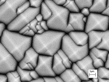
1.Carbon nanotubes as electrical interconnects and thermal interface materials
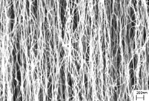
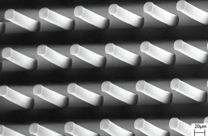
Our interests focus on synthesis, fabrication and characterization of carbon nanotubes for applications as electrical interconnects and thermal interface materials in the filed of electronic packaging. Via optimization of the catalyst composition and the CVD recipe, we devote to synthesize CNTs of outstanding properties, high alignment and packing density. In terms of realization of the true potential of CNTs, the bottle neck is currently the electron transport, phonon transport and stress transer at heterogeneous juctions at CNT/substrate or CNT/polymer matrix interfaces. We aim at providing an insightful interface design, based on fundamentals in chemistry and physics, to address these challenging issues.
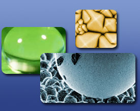
2.Superhydrophobic, oleophobic, self-cleaning surfaces for high efficiency photovoltaic applications
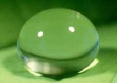
Lotus effect surfaces offer much promise for the formation of high-performance micro-/nano-structured surfaces with multifunctionality that can be used in optical, photoelectric, microelectronic, catalytic, and biomedical applications. The overall goal for the project is to prepare non-reflecting, self-cleaning, moisture repellent surfaces to prevent the degradation of solar cell efficiency based on Lotus Effect technology. By using different etching methods, we will study the structure geometry effect on superhydrophobicity and oleophobicity, and investigate the effect of controlled silicon surface texture on light reflection and light trapping in solar cells.
3.Introduction of ECAs
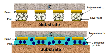 Fig. 1 Schematic representation of ICA and ACA/ACF joints
Electrically conductive adhesives (ECAs) have been considered as the most promising
alternatives of tin-lead solder. ECAs consist of a polymeric resin (such as, an
epoxy, a silicone, or a polyimide) that provides physical and mechanical properties
such as adhesion, mechanical strength, impact strength, and metal fillers (such
as, silver, gold, nickel or copper) that conducts electricity. ECA can be categorized
with respect to conductive filler loading level into anisotropically conductive
adhesives (ACAs/ACFs) and isotropically conductive adhesives (ICAs), as shown in
Fig. 1. ECAs offer numerous advantages over conventional solder technology, such
as environmental friendliness, mild processing conditions (enabling the use of heat-sensitive
and low-cost components and substrates), fewer processing steps (reducing processing
cost), low stress on the substrates, and fine pitch interconnect capability (enabling
the miniaturization of electronic devices).
In recognition of the importance and issues of ECAs, we have extensively studied
and been continuously working on:
- conduction mechanism of ECAs
- the dominant mechanisms underlying the unstable contact resistance of ECAs
- considerable enhancements of electrical properties by using nano-scale conductive materials (such as Ag nanoparticles and carbon nanotubes) and conjugated molecular wires
- Ag migration control
- physical/chemical properties of epoxy resins
- adhesion strengths of ECAs on different surface finish such as Ni/Au, Cu, etc.
- development of flexible and transparent ECAs
- high frequency properties of ECA-based joints
- development of highly reliable low-cost Cu-based ECAs
- jet dispensing of ECAs, etc. Our objective is to gain the fundamental understanding of ECAs and develop ECAs for high-performance fine-pitch interconnection applications.
4.graphene
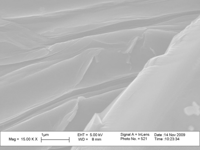 SEM images of GO
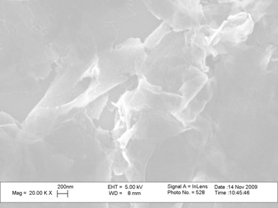 SEM images of reduced GO
Our research focuses on the controlled synthesis, fabrication and characterization of graphene for applications of advanced electrical materials, such as high performance electrode material in high power/energy density ultracapacitors. We devote to understand fundamental aspects on the graphite exfoliation and graphene oxide reduction which is essential to tune the structure of graphene and also packaging of graphene. We aim to control the size, number of layers, and degree of functionalization et al. of graphene, and thus the surface area, stability and electrical conductivity, to optimize its performance.
5.Electronic packaging coating and encapsulation materials
The coating subgroup is interested to provide better electronic packaging technology by novel composite or nanomaterials. Current projects include the underfill materials for the flip chip connection and aging sensors for electronics.